
PHINDER / Technology
Technology
Nanowire neurons. Optical connections. Integrated intelligence.
PHINDER investigates how III–V nanowire devices and indium-phosphide (InP) photonic integrated circuits can form a sensing and processing platform. The technology combines local optoelectronic computation with optical links and programmable photonic networks.
01 / Devices and connections
Nanoscale optoelectronic building blocks
Semiconductor nanowires can act as photodetectors, light emitters, transistors and wavelength-selective optical elements. Their small footprint brings detection, signal integration and activation close together. Deterministic placement and fabrication techniques allow different nanowires to be positioned and contacted in designed circuits.
Light connects the nodes
Flodgren and colleagues demonstrated direct on-chip optical communication between individual nanowire devices. Light from an emitter reaches a neighbouring receiver without an electrical signal wire connecting the two.
This makes geometry and optical properties part of the computing architecture. Optical-broadcasting research explores how nanowire position, orientation and wavelength affect coupling and network connectivity.
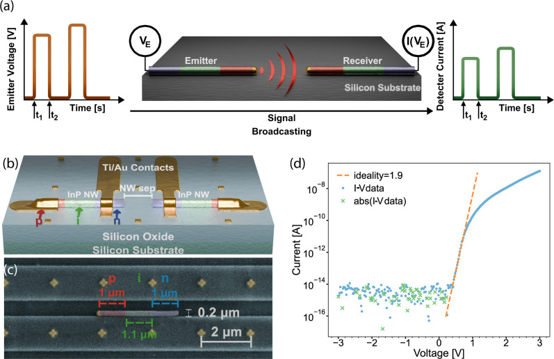
From an optical link to a fabricated device. The published figure brings together the broadcasting principle, nanowire circuit, microscopy and electrical characterisation. View full size ↗
Figure 1 from Flodgren et al., ACS Photonics (2025). · CC BY 4.0
02 / Heterogeneous integration
Photonic integration for larger networks
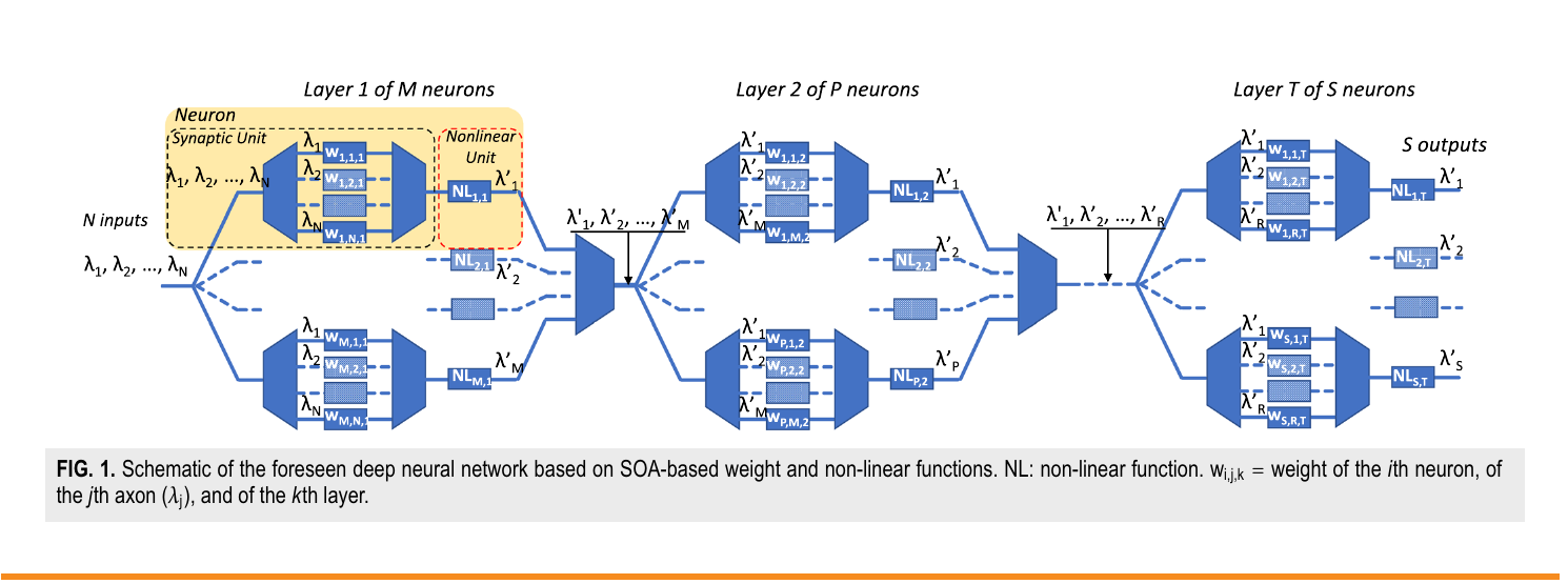
PHINDER will investigate integration of III–V nanowire nodes with InP photonic integrated circuits. Waveguides, wavelength-division multiplexing and optical fan-out provide routes to distribute signals among many nodes. Semiconductor optical amplifiers and nonlinear stages can support weighted connections and processing on chip.
The InP multilayer-network architecture of Shi, Calabretta and Stabile provides relevant background for this approach. It describes a photonic network architecture and performance analysis, rather than an already completed PHINDER circuit.
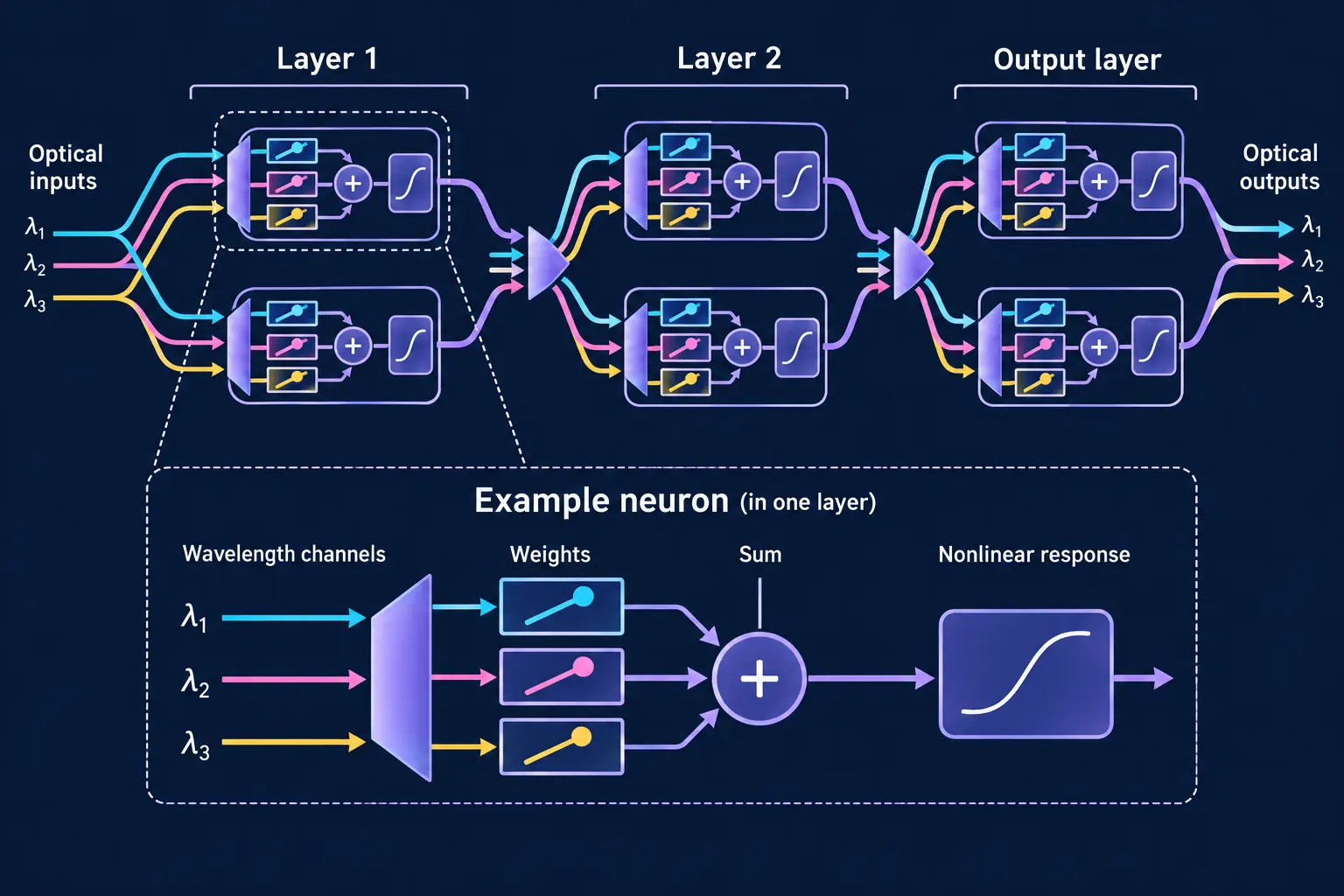
Wavelength channels, weighted connections and nonlinear stages form a route to multilayer InP photonic networks. The architecture is simplified here to show the signal flow. View full size ↗
Simplified AI-assisted redraw of Figure 1 from Shi, Calabretta and Stabile, APL Photonics (2022). · CC BY 4.0 · Original figure
03 / Hardware–algorithm co-design
Co-designed from device to application
The physical device, photonic network and learning algorithm cannot be optimised independently. PHINDER combines component models, system-level digital twins and application simulations. Measurements from fabricated prototypes will feed back into the models and algorithms.
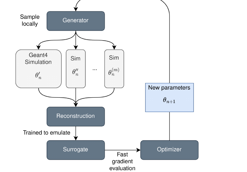
A surrogate model learns to emulate an expensive simulation and reconstruction chain. It can then accelerate exploration of design choices and provide gradients for optimisation. The AIDO workflow illustrates this iterative approach for detector design; robustness-oriented photonic training adds complementary background on hardware-aware optimisation.
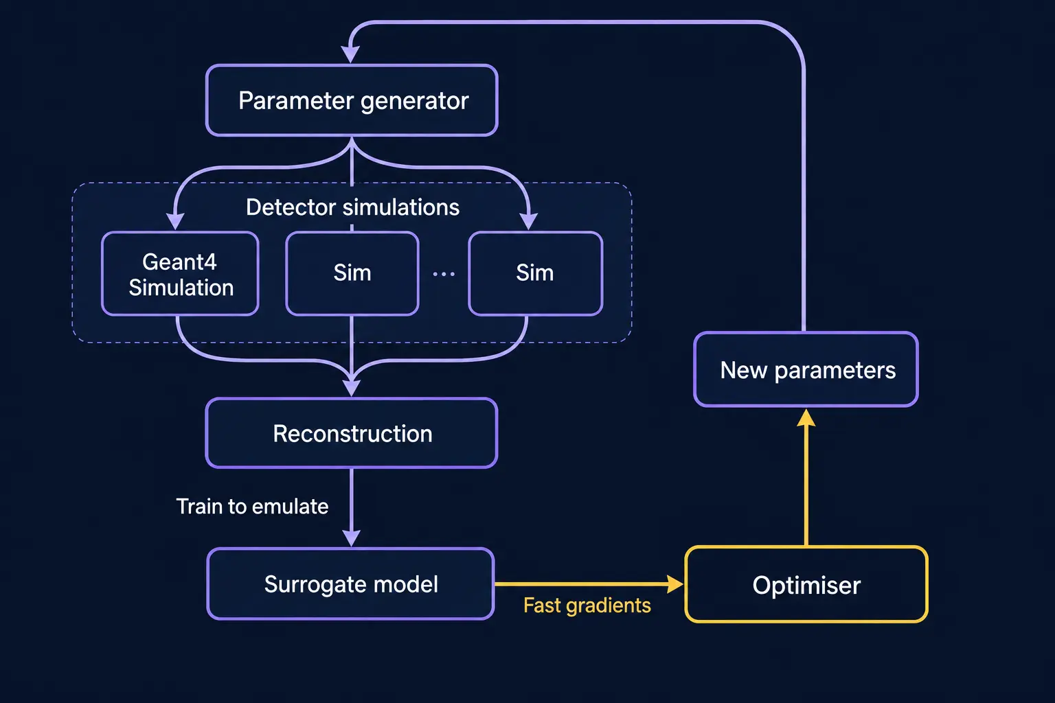
A learned surrogate emulates the simulation and reconstruction chain, enabling fast gradient evaluation as an optimiser proposes the next design parameters. View full size ↗
Simplified AI-assisted redraw of Figure 2 from Schmidt et al., Particles (2025). · CC BY 4.0 · Original figure
Research objectives
The project targets picosecond-scale optical event detection, sub-nanosecond latency and improved energy efficiency through closely coupled sensing and processing. These are research objectives, not specifications of an available device.
Read the relevant background publications →
Code and collaboration
Follow the consortium’s software and development activity on PHINDER’s GitHub organisation.
Opportunities
The previously advertised Oviedo and Cantabria PhD calls have closed. Future opportunities will be announced here and in the news.